1. Introduction.
I'm one of those hobbyists, who moved out of doing Arduino projects (and some other pre-built boards) into making my own boards. I started from simple two-layer boards with MCU and some peripheral chips - which were essentially a "condensed" version of Arduino projects. But as it tends to happen to a lot of engineers, with each successful board design excitement from getting it to work fades away, and so craving for that euphoric burst of excitement when newly assembled board comes to life for the first time demands making more and more complicated designs. It's that craving that drives many hobbyists like me to march on, and on, and on. That's what shifted my attention to FPGA. FPGA projects seems like a Holy Grail for electronic engineers-hobbyists, as it's the closest thing to designing your very own ICs the regular person like can get to without having few million dollars to spend on a hobby. But most FPGA chips nowadays are only available in BGA packages, and routing high speed lines requires at least four-layer boards to achieve needed trace impedance anyway.
This brings us to the essence of the problem - the price of manufacturing such boards. While 4-layer boards with 0.15 mm traces/0.15 mm spacing and 0.3 mm drills have recently become very affordable, they are only good for breaking out BGAs with 1.0 mm ball pitch. But many modern ICs - things like DDR2/3 memory, pretty much all more-or-less modern microprocessors, system-on-chip ICs - are only available in 0.8 mm ball pitch BGA packages (or even finer), and reliably breaking them out requires using more advanced PCB manufacturing process with 0.1 mm trace/0.1 mm spacing and 0.2 mm drills, not to mention that really high-speed traces (like DDR2/3, USB 2/3, HDMI and many other) require controlled impedance. And as soon as you ask for any of these things, the cost of manufacturing skyrockets!
2. The mission.
And so I set myself out on a mission to find a PCB fab, which would be able to manufacture boards with 0.1/0.1 mm trace/spacing and 0.2 mm min drill at affordable price. Somewhat arbitrarily I set myself a limit of $250 for ten 6-layer boards 10x10 cm, and $180 for ten 4-layer boards 10x10 cm. These prices have to include ENIG finish (as soldering BGAs onto boards with cheaper HASL has proved to be a hit-n-miss affair, and I didn't want to gamble with chips that costs a lot of money), 10 business days of lead time (or less), and express shipping to my door.
That kind of restriction immediately disqualified all US, Canada and Europe-based manufacturers, as some of them would charge that much for even simple two-layer boards. And so I went into Google and started searching. During the search I've skipped all PCB fabs which did not publish their prices as that usually indicates that they are going to be high. This is my personal position - if company is afraid to publish their prices, it likely means that it's afraid to scare potential customer away before sales rep has a chance to "size him up" and figure out what kind of price he is likely to be willing to pay. Thankfully, many PCB houses nowadays have some kind of instant online quoting system that allows user to "dial in" whatever requirements he has, and see the price.
I have to say that I successfully used
PCBWay and
Allpcb services many times for my two-layer boards projects, so naturally I went there and checked their pricing. However the former's online quoting system quoted me $341 for that kind of order, and the latter doesn't do 0.1 traces and 0.2 drills at all, and my inquiries via email were not answered.
3. First contact.
This is how I found
OurPCB. Their website is fairly typical for China-based PCB fab - simple design, dodgy at times English. But what interested me is
this page, which lists prices that are almost too good to be real. Unfortunately there is no online quoting system there, but published prices were so good that I decided to break my own rule of "no email inquiries" and sent them an email asking for the quote.
Next morning I received an email asking me to provide Gerber files for the board I want to manufacture. This was not unexpected, but after few rounds of back-end-forth I explained that I don't want to start designing the board until I receive the quote that would be affordable for me. I also needed to know the stackup they use as well as material properties so that I can calculate trace width for traces with controlled impedance. Finally he sent me the quote for $234! And he told me that I can design whatever stackup I want! THIS is a BIG deal!! Many PCB designers know that for the reason that escapes me fabs tend to have "standand" stackups that are not very useful for modern hi-speed designs, and they will charge through the nose if you request a custom stackup. While this fab just flat out said "we can manufacture whatever stackup you want without extra costs to you". Just WOW!
4. The design.
And so I went on to design the board. I wanted to design a devboard which would contain DDR3 x16 memory chip, Artix-100 (or any smaller pin-compatible) FPGA in BGA-256 package, FT601 USB3-to-parallel bus bridge IC, as well as having connectors for HDMI TX, and parallel LCD screen with capacitive touchscreen and a boost DC-DC converter for LCD backlight. And of course some LEDs (settled on a pair of RGB LEDs), buttons and switches for debugging. This consumed pretty much all FPGA IO pins.
I don't want to get too much into details of this design as this would be better done in a separate post, and if there will be interest in it, I can write it up. For now the important thing is that it is a 6-layer boards with traces/spacing down to 0.1 mm (though only in BGA breakout areas, traces are thicker elsewhere), and 0.2 mm minimum drills.
To design the stackup, I've searched around a bit for standard material sizes that are commonly used, and used information from
this page as a guide. Here is the stackup I've settled on:
My personal big problem is that I almost never managed to get my boards 100% right on a first try, so this time I went an extra mile to raise my chances (as $200+ is a big amount of money to throw away due to some stupid mistake on my part!), so I've printed the top layer with holes and routes on a paper, and checked that all major parts and connectors would match their PCB footprints - and not surprisingly, I ended up having to fix some of them!
After all these corrections and rounds of verification I felt confident enough to declare it completed and sent it for fabrication. I received the final quote for $237.33. A day after I paid it (I didn't bother asking why the price was adjusted as the change was so small), I received an email from sales rep's assistant with some questions, as well as production files and the stackup and controlled impedance traces calculations for my approval. Here is the stackup they ended up fabricating:
as you can see, it's pretty much spot-on to what I requested (to within 0.01 mm!). I checked the files (they turned out to be correct), answered all questions, and approved fabrication.
5. The wait.
Well this is the worst part of the business. I don't know about other engineers, but I totally hate this part! In order to fill the time, I decided to export the BOM and figure out which parts will I need to order to assemble the board. In should be said, that in order to fit decoupling caps between FPGA breakout vias, I've decided to use 0.47 uF caps in tiny 0201 package, so I expected to see them in BOM as the only 0201 part. And that when first issue surfaced - much to my horror, I've found out that I have not one, but four! different values of 0201 caps! Frantically I went on to see where exactly did I place these things, and to my relief, found out that they were only in low-voltage lines, and values ended up being such that these parts actually do exist. Another issue I've discovered is that I forgot to include a termination resistor for DDR3 clock line, but after looking at layout for places where I can hack it in and running some IBIS simulations to determine the best place among them, I've concluded that it would be best to solder it to breakout vias under memory IC - as luck would have it, these two vias are placed diagonally relative to each other within 0.8 mm breakout grid, and so the distance between them would be sqrt(0.8^2 + 0.8^2)~1.13 mm - more than enough to solder 0402 resistor (it's length is about 0.1 mm).
6. Delivery.
This Monday's morning I woke up and found an email from the fab notifying me that they've shipped out my order. Initially DHL was supposed to deliver it on Wednesday, but they managed to lose my package somewhere between their depot and the dropff location that I always used for DHL deliveries. I called them on Thursday, and eventually they told me that it might take up to 48 hours to locate the shipment. I was furious as I just managed to free up the weekend so that I can at least partially assemble the board (I plan to assemble just power-related portion on the first board to verify that all voltages are what they should be, and if they won't be - sort this out without risk of killing expensive ICs in the process. After that, the next board will be fully assembled - albeit will smaller FPGA just in case I messed up something else in layout. Assuming all this will check out, only the third board will be assembled fully with Artix-100 FPGA and all the rest). Anyhow, DHL contacted me today (on Friday) and informed me that they found the parcel and dispatched it to the dropoff location, and it should be available for pickup in the evening. And it was - hence this post :)
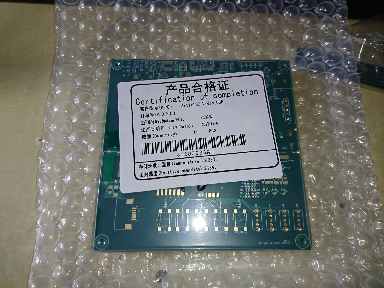
7. The package.
After making my way home I immediately set out to open the box to see what I got. It arrived in a typical well-packaged box, filled with foam:
And here was the first surprise - they've sent me the coupon and a cross-section of the board - even though I didn't specifically ask for it! There was also a five pages long QA report, which included, among other things, materials report, verification of materials, features' dimensions, electrical test (including high-voltage insulation test), microsection analysis, solderability test, thermal stress test, and CI traces impedance test! Again - they did all of this out of their own accord, I only requested flying probe test. Outstanding! I didn't bother scanning reports, but if anyone is interested to see them - please let me know and I will scan and post them.
Actual boards were packaged in vacuum-sealed bubble packaging, which is typical:
8. The board.
Now let's get to the meat of this post - the board. This is what it looks like:
 |
| Front side |
 |
| Back side |
I'm positively impressed by the silkscreen quality - even very small 0.64 mm high characters are quite readable! But let's take a closer look under microscope!
 |
| Main FPGA footprint |
 |
| DDR3 x16 footprint |
 |
| HDMI connector footprint (note presence of soldermask between pins despite 0.5 mm pitch with only 0.2 mm airgap between pins!) |
 |
| FT601 footprint (again solder stops are there despite even smaller 0.4 mm pin pitch and only 0.18 mm of airgap) |
 |
| FT601 footprint (again solder stops are there despite even smaller 0.4 mm pin pitch and only 0.18 mm of airgap) |
 |
| 12 V to 5 V DC-DC converter in very small QFN package |
 |
| Main 4-channel PMIC in QFN package (again - nothing to write home about, just perfect quality) |
 |
| 0.5 mm pitch 40-pin connector for LCD panel (left) and some serial termination 4-resistor networks in 0804 packages (right) |
 |
| 0.5 mm pitch 40-pin connector for LCD panel (left) and some serial termination 4-resistor networks in 0804 packages (right) |
 |
| Tiny 0201 capacitors as part of 5 Gbps USB3 TX differential pair |
 |
| Solder bridges to adapt board for different LCD panels |
 |
| Footprint for SPI Flash in 1 mm ball pitch BGA-24 package |
 |
| A sea of 0201 and 0402 decoupling caps under FPGA |
 |
| Exposed pad under main PMIC in case I will need to mount a heatsink |
 |
| Left - power jack with input capacitor, right - exposed pad of 12-to-5 V DC-DC converter in case I need to add a heatsink |
 |
| Screw-up of the day - outline is on a solder mask layer instead of silk screen |
 |
| Screw-up of the day - outline is on a solder mask layer instead of silk screen |
 |
| Cross-section photo |
 |
| Cross-section photo |
 |
| Cross-section photo |
It has to be said that OurPCB engineer noticed the screwup with connector, but I misunderstood him at the time, and only today realized what he was telling me :(.
9. Conclusion.
Well it should be fairly obvious by now what do I think of this fab at this point. The boards are some of the best-quality I've ever seen (which isn't telling a lot, but still...), I visually inspected the board under x20 stereo microscope and didn't find a single thing to complain about. The price is good. The lead time is adequate.
I don't know if boards will actually work at this point, but even if they won't I'd be inclined to think that it's my own fault rather than that of the fab, so I absolutely and totally recommend to give them a try if you're like me on a market for affordable 6-layer boards! I will post updates as I assemble boards, but for now I'm checking out. Thank you for taking time to read though all of this!
Disclaimer: I am NOT affiliated with OurPCB in any way, shape or form. I will NOT receive any kind of compensation, discount, award or anything else for this review. Everything written above is a reflection of this order and this order alone, so your experience may be different.